Introduction
JP1 (Jumper 1)
Determines AD526 (gain control factor) is used.
JP2 (Jumper 2)
Determines AD526 (gain control factor) is used.
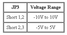
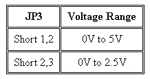
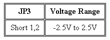
JP3 (Jumper 3)
Determine A/D voltage range.
JP4 (Jumper 4)
Determines D/A voltage range for channel 1.
JP5 (Jumper 5)
Determines D/A voltage range for channel 2.
JP6 (Jumper 6)
Determines unipolar or bipolar for D/A channel 1.
JP7 (Jumper 7)
Determines unipolar or bipolar for D/A channel 2.
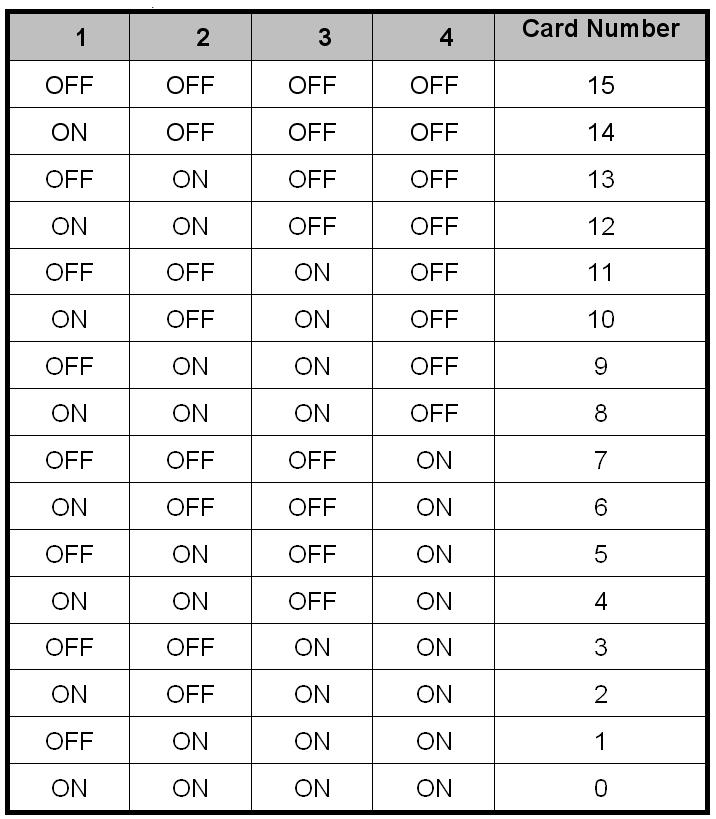
SW1 (Switch 1)
Identifies card number.
| 1. | I/O Port Address |
| The plug and play features set I/O port address automatically, please refer the device manager of control panel to get base port address of this adapter. | |
| 2. | Voltage Range of D/A Channel |
JP4 is used to select a range of output
voltage for D/A channel 1, and JP5 is used to select a range of output
voltage for D/A channel 2. JP6 is used to select unipolar or bipolar of
D/A channel 1, and JP7 is used to select unipolar or bipolar of D/A
channel 2.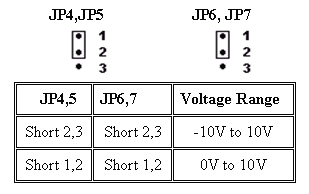 |
|
| 3. | Voltage Range of A/D Channel |
| |
JP3 is used to select input voltage range for
A/D channel. There are several kinds of A/D chip can be plug in
adapter. For different A/D chip, the voltage range and
unipolar/bipolar setting are difference. |
| (1)
For AD7899AR-1 chip Voltage range : -5V to +5V
or –10V to +10V +/-2LSB
Temperature : -40 to 85C
 |
|
| |
(2)
For AD7899AR-2 chip Voltage range : 0V to +2.5V
or 0V to +5V +/-2LSB
Temperature : -40 to 85C
 |
| (3)
For AD7899AR-3 chip Voltage range : -2.5V to
+2.5V +/-2LSB
Temperature : -40 to 85C
 |
|
| 4. | Input Mode for AD7899 |
| The JP2
is used to adjust input offset of AD7899. Setting the jumper to pin 2
and pin 3 will ground the input value (0V), so the data that will be
converted should also be 0. Shorting jumper to pin 1 and pin 2 will make use of the channel inputs to be read and converted. It is the normal input mode. 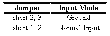 |
|
| 5. | Programmable Gain Control Factor (AD526) |
The JP1 is used to select programmable gain
control factor, when not short the jumper, it enable AD526, otherwise
short the pin means no AD526 work (can not control gain control factor).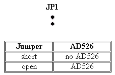 |
|
| 6. |
Card Identifier 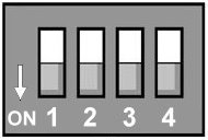
|
For READ input
port + 0: input 14 bit A/D data.
port + 2: clear the interrupt signal that generated from the adapter.
port + 6: 16 bit digital signal input.
port + 8: counter 0 I/O buffer (8254 IC).
port + 9: counter 1 I/O buffer (8254 IC).
port + A: counter 2 I/O buffer (8254 IC).
port + B: counter control register (8254 IC).
For WRITE output
port + 0: select A/D channel number, enable/disable the selected channel, select IRQ and select control method.
port + 2: 14 bit D/A channel 1.
port + 4: 14 bit D/A channel 2.
port + 6: 16 bit digital output.
port + 8: counter 0 I/O buffer (8254 IC).
port + 9: counter 1 I/O buffer (8254 IC).
port + A: counter 2 I/O buffer (8254 IC).
port + B: counter control register (8254 IC).
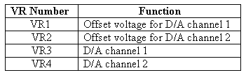
VR1 is used to adjust the D/A channel 1 offset voltage, and VR2 is used to adjust the D/A channel 2 offset voltage. In the following, we describe offset adjust.
To adjust D/A channel 1 offset voltage, please follow the step shown in the below:
Step 1: for min voltage, short pin 2 and pin 3 of JP4, and pin 2 and pin 3 of JP6, then adjust VR3 to let J1-15 output voltage to –10V. If the error rate more than 1.2mV, please enter step 2 to adjust VR1 for offset voltage.
Step 2: for middle voltage, short pin 2 and pin 3 of JP4, and pin 2 and pin 3 of JP6, then adjust VR1 to let J1-15 output voltage to 1.2mV.
Step 3: for max voltage, short pin 2 and pin 3 of JP4, and pin 2 and pin 3 of JP6, then adjust VR3 to let J1-15 output voltage to 10V. If the error rate more than 1.2mV, please enter step 2 to adjust VR1 for offset voltage.
To adjust D/A channel 2 offset voltage, please follow the step shown in the below:
Step 1: for min voltage, short pin 2 and pin 3 of JP5, and pin 2 and pin 3 of JP7, then adjust VR4 to let J1-3 output voltage to –10V. If the error rate more than 1.2mV, please enter step 2 to adjust VR2 for offset voltage.
Step 2: for middle voltage, short pin 2 and pin 3 of JP5, and pin 2 and pin 3 of JP7, then adjust VR2 to let J1-3 output voltage to 1.2mV.
Step 3: for max voltage, short pin 2 and pin 3 of JP5, and pin 2 and pin 3 of JP7, then adjust VR4 to let J1-15 output voltage to 10V. If the error rate more than 1.2mV, please enter step 2 to adjust VR2 for offset voltage.
| 1. | A/D and D/A loopback test |
| 2. | D/A output test |
| 3. | A/D input test |
| 4. | DIO loopback test |
| 5. | DIO output test |
| 6. | DIO input test |
| 7. | D/A calibration |
| Pin |
Function |
Pin |
Function |
| 1 |
+ 12 V |
14 |
-12 V |
| 2 |
/EXTRG |
15 |
D/A
channel 1 |
| 3 |
D/A
channel 2 |
16 |
CH15 |
| 4 |
CH14 |
17 |
CH13 |
| 5 |
CH12 |
18 |
CH11 |
| 6 |
CH10 |
19 |
CH9 |
| 7 |
CH8 |
20 |
CH7 |
| 8 |
CH6 |
21 |
CH5 |
| 9 |
CH4 |
22 |
CH3 |
| 10 |
CH2 |
23 |
CH1 |
| 11 |
CH0 |
24 |
GND |
| 12 |
GND |
25 |
|
| 13 |
+5 V |
| Pin |
Function |
Pin |
Function |
| 1 |
14 |
GND |
|
| 2 |
+12V |
15 |
GND |
| 3 |
D8 |
16 |
D9 |
| 4 |
D10 |
17 |
D11 |
| 5 |
D12 | 18 |
D13 |
| 6 |
D14 | 19 |
D15 |
| 7 |
D0 | 20 |
D1 |
| 8 |
D2 | 21 |
D3 |
| 9 |
D4 | 22 |
D5 |
| 10 |
D6 | 23 |
D7 |
| 11 |
24 |
||
| 12 |
+5V |
25 |
GND |
| 13 |
-12V |
26 |
GND |